
Author Affiliations
Abstract
1 Center for Terahertz Waves and College of Precision Instrument and Optoelectronics Engineering, Tianjin University and the Key Laboratory of Optoelectronics Information and Technology (Ministry of Education), Tianjin 300072, China
2 Guangxi Key Laboratory of Optoelectronic Information Processing, School of Optoelectronic Engineering, Guilin University of Electronic Technology, Guilin 541004, China
3 School of Electronic and Computer Engineering, Oklahoma State University, Stillwater, OK 74078, USA
Plasmonic vortices confining orbital angular momentums to surface have aroused wide research interest in the last decade. Recent advances of near-field microscopes have enabled the study on the spatiotemporal dynamics of plasmonic vortices, providing a better understanding of optical orbital angular momentums in the evanescent wave regime. However, these works only focused on the objective characterization of plasmonic vortex and have not achieved subjectively tailoring of its spatiotemporal dynamics for specific applications. Herein, it is demonstrated that the plasmonic vortices with the same topological charge can be endowed with distinct spatiotemporal dynamics by simply changing the coupler design. Based on a near-field scanning terahertz microscopy, the surface plasmon fields are directly obtained with ultrahigh spatiotemporal resolution, experimentally exhibiting the generation and evolution divergences during the whole lifetime of plasmonic vortices. The proposed strategy is straightforward and universal, which can be readily applied into visible or infrared frequencies, facilitating the development of plasmonic vortex related researches and applications.
plasmonic vortex surface plasmon spatiotemporal dynamics optical orbital angular momentum Opto-Electronic Advances
2023, 6(4): 220133

Author Affiliations
Abstract
1 Center for Terahertz Waves and College of Precision Instrument and Optoelectronics Engineering, Key Laboratory of Optoelectronic Information Technology (Ministry of Education of China), Tianjin University, Tianjin 300072, China
2 School of Optoelectronic Engineering and Instrumentation Science, Dalian University of Technology, Dalian 116024, China
3 Georgia Tech Shenzhen Institute (GTSI), Tianjin University, Shenzhen 518067, China
4 e-mail: caotun1806@dlut.edu.cn
High-performance terahertz (THz) devices with reconfigurable features are highly desirable in many promising THz applications. However, most of the existing reconfigurable THz elements are still limited to volatile responses, single functionality, and time-consuming multistep manufacturing procedures. In this paper, we report a lithography-free approach to create reconfigurable and nonvolatile THz components by exploring the reversible, nonvolatile, and continuous THz modulation capability of the phase change material . As a proof of concept, THz gratings with significant Rayleigh anomalies and diffraction as well as ultrathin THz flat lenses with subwavelength and ultra-broadband focusing capabilities are designed and fabricated on ultrathin films using the presented photo-imprint strategy. Moreover, such a method can also be adopted to create more complex THz devices, such as Pancharatnam–Berry phase metasurfaces and grayscale holographic plates. With these findings, the proposed method will provide a promising solution to realize reconfigurable and nonvolatile THz elements.
Photonics Research
2023, 11(4): 669

Author Affiliations
Abstract
1 Center for Terahertz Waves and College of Precision Instrument and Optoelectronics Engineering, Key Laboratory of Optoelectronic Information Technology (Ministry of Education), Tianjin University, Tianjin, China
2 Guangxi Key Laboratory of Optoelectronic Information Processing, Guilin University of Electronic Technology, Guilin, China
3 School of Electrical and Computer Engineering, Oklahoma State University, Stillwater, USA
Surface plasmons (SPs) are electromagnetic surface waves that propagate at the interface between a conductor and a dielectric. Due to their unique ability to concentrate light on two-dimensional platforms and produce very high local-field intensity, SPs have rapidly fueled a variety of fundamental advances and practical applications. In parallel, the development of metamaterials and metasurfaces has rapidly revolutionized the design concepts of traditional optical devices, fostering the exciting field of meta-optics. This review focuses on recent progress of meta-optics inspired SP devices, which are implemented by the careful design of subwavelength structures and the arrangement of their spatial distributions. Devices of general interest, including coupling devices, on-chip tailoring devices, and decoupling devices, as well as nascent SP applications empowered by sophisticated usage of meta-optics, are introduced and discussed.
surface plasmons metamaterials metasurfaces plasmonics metadevices Photonics Insights
2023, 2(1): R02
Author Affiliations
Abstract
1 Center for Terahertz Waves and School of Precision Instrument and Optoelectronics Engineering, Key Laboratory of Optoelectronic Information Technology (Ministry of Education of China), Tianjin University, Tianjin 300072, China
2 School of Optoelectronic Engineering and Instrumentation Science, Dalian University of Technology, Dalian 116024, People’s Republic of China
3 Georgia Tech Shenzhen Institute (GTSI), Tianjin University, Shenzhen 518067, China
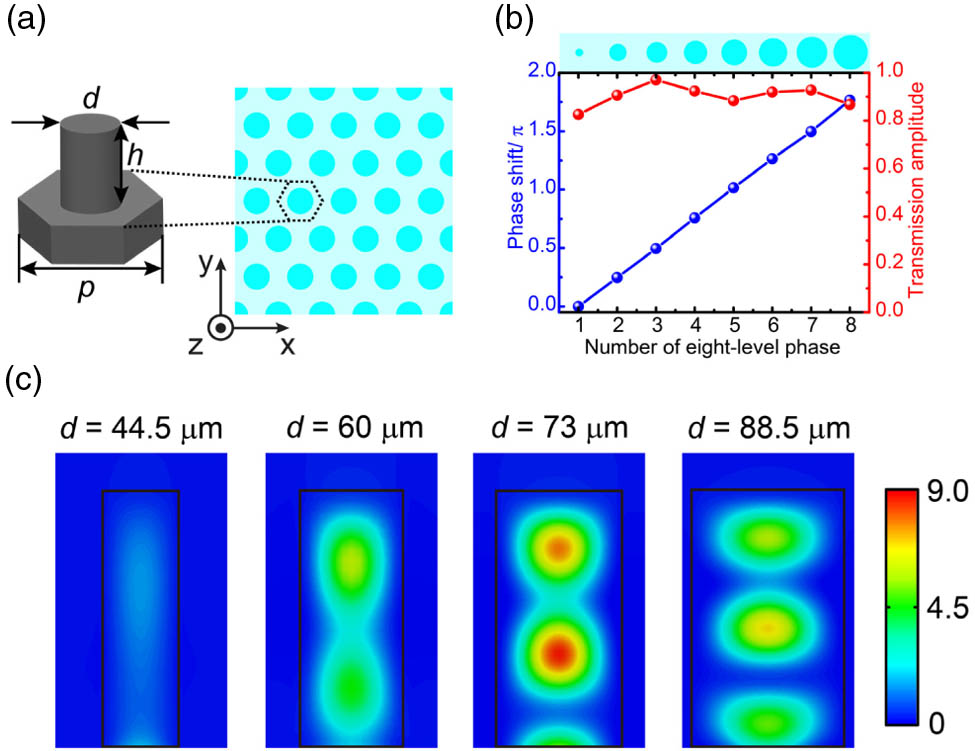
Miniaturized nonvolatile reconfigurable optical components with a subwavelength thickness, extremely compact size, high-speed response, and low power consumption will be the core of next-generation all-optical integrated devices and photonic computing to replace traditional bulky optical devices and integrated circuits, which are reaching physical limitations of Moore’s law. Metasurfaces, as ultrathin planar surfaces, have played a major role in controlling the amplitude, phase, and polarization of electromagnetic waves and can be combined with various active modulation methods to realize a variety of functional devices. However, most existing reconfigurable devices are bounded in volatile nature with constant power to maintain and single functionality, which restricts their further extensive applications. Chalcogenide phase change materials (PCM) have attracted considerable attention due to their unique optical properties in the visible and infrared domains, whereas in the terahertz (THz) regime, research on the reversible phase transition in large-scale areas and applications of Ge2Sb2Te5 (GST) are still under exploration. Here, we achieved reversible, repeated, and large-area switching of GST with the help of optical and thermal stimuli. Large-area amorphization with a 1 cm diameter of GST is realized by using a single laser pulse. Then, we incorporate GST into metasurface designs to realize nonvolatile, reconfigurable, multilevel, and broadband terahertz modulators, including the anomalous deflector, metalens, and focusing optical vortex (FOV) generator. Experimental results verify the feasibility of multilevel modulation of THz waves in a broadband frequency range. Moreover, the modulators are reusable and nonvolatile. The proposed approach presents novel avenues of nonvolatile and reconfigurable metasurface designs and can enable wide potential applications in imaging, sensing, and high-speed communications.

Author Affiliations
Abstract
1 Center for Terahertz Waves and College of Precision Instrument and Optoelectronics Engineering, Key Laboratory of Optoelectronic Information Technology (Ministry of Education of China), Tianjin University, Tianjin 300072, China
2 School of Optoelectronic Engineering and Instrumentation Science, Dalian University of Technology, Dalian 116024, China
3 Georgia Tech Shenzhen Institute (GTSI), Tianjin University, Shenzhen 518067, China
4 e-mail: caotun1806@dlut.edu.cn
5 e-mail: tianzhen@tju.edu.cn
Metasurfaces, especially tunable ones, have played a major role in controlling the amplitude, phase, and polarization of electromagnetic waves and attracted growing interest, with a view toward a new generation of miniaturized devices. However, to date, most existing reconfigurable devices are bounded in volatile nature with sustained external energy to maintain and single functionality, which restrict their further applications. Here, we demonstrate for the first time, to our knowledge, nonvolatile, reconfigurable, and dynamic Janus metasurfaces by incorporating phase-change material (GST) in the terahertz (THz) regime. First, we experimentally show the reversible switching characteristic of GST on large areas by applying a single nanosecond laser pulse, which exhibits excellent contrast of THz properties in both states. Then, we present a multiplex metasurface scheme. In each metasurface, three sets of structures are adopted, in which two sets integrate GST. The effective structures can be reversely modulated by the amorphization and crystallization of GST. As a proof of concept, the dynamic beam splitter, bifocal metalens, dual-mode focusing optical vortex generators, and switchable metalens/focusing optical vortex generators are designed, fabricated, and experimentally characterized, and can be switched reversibly and repeatedly with the help of optical and thermal stimuli. Our scheme will pave the way toward the development of multifunctional and compact THz devices and may find use for applications in THz imaging, sensing, and communications.
Photonics Research
2022, 10(7): 1731

Author Affiliations
Abstract
1 Center for Terahertz Waves and College of Precision Instrument and Optoelectronics Engineering, Tianjin University, and Key Laboratory of Optoelectronics Information and Technology, Ministry of Education of China, Tianjin 300072, China
2 Cavendish Laboratory, University of Cambridge, Cambridge CB3 0HE, UK
3 Guangxi Key Laboratory of Optoelectronic Information Processing, School of Optoelectronic Engineering, Guilin University of Electronic Technology, Guilin 541004, China
4 e-mail: hz372@cam.ac.uk
5 e-mail: alearn@tju.edu.cn
6 e-mail: heb1000@cam.ac.uk
7 e-mail: jiaghan@tju.edu.cn
Metasurfaces consisting of artificial subwavelength structure arrays have shown unprecedented ability to manipulate the phase, amplitude, and polarization of light. Separate and complete control over different spin states, namely the orthogonal circular polarizations, has proven more challenging as compared to the control over orthogonal linear polarizations. Here, we present and experimentally demonstrate several spin-dependent wavefront control metasurfaces in the terahertz regime using all-silicon dielectric structures. Such spin-dependent all-silicon metasurfaces are easy to fabricate and have potential applications in spin-involved ultracompact and miniaturized terahertz optical systems as well as terahertz communication systems.
Photonics Research
2022, 10(7): 07001695
天津大学精密仪器与光电子工程学院太赫兹研究中心,天津 300072
全息术是一种三维成像技术,它已经被应用于多种实际场景。随着计算机科学与技术的迅猛发展,计算全息由于其方便和灵活的特性,已经成为一种广泛应用的全息成像方法。本文回顾了我们近期基于超表面的太赫兹计算全息研究进展。其中,作为全息板的超表面展示出了超越传统光学器件的独特性能。首先,利用超表面实现了对于全息板每个像素的相位振幅同时且独立的调控,进而实现了高质量全息成像。这种新的电磁波操控能力也带来了新的全息成像效果,如利用介质超表面实现了全息像沿传播方向上的连续变化。其次,对超表面在不同偏振态下的响应进行设计,分别实现了线偏振态与频率复用、圆偏振态复用、以及基于表面波的偏振复用超表面全息术。此外,本文提出了依赖于温度变化而主动可控的超表面全息术,为今后计算全息术的设计与实现提供了新的方案,也推动了超表面在实际应用方面的发展。
太赫兹 计算全息 超表面 多路复用 terahertz computer generated holography metasurface multiplexing

Author Affiliations
Abstract
1 Center for Terahertz Waves and College of Precision Instrument and Optoelectronics Engineering, Tianjin University, and the Key Laboratory of Optoelectronics Information and Technology Tianjin, Ministry of Education of China, Tianjin 300072, China
2 Physical Science and Engineering Division, King Abdullah University of Science and Technology, Thuwal 23955-6900, Saudi Arabia
3 Division of Physics and Applied Physics, School of Physical and Mathematical Sciences, Nanyang Technological University, 21 Nanyang Link, Singapore 637371, Singapore
4 Research Institute of Superconductor Electronics (RISE), School of Electronic Science and Engineering, Nanjing University, Nanjing 210093, China
5 School of Electrical and Computer Engineering, Oklahoma State University, Stillwater, Oklahoma 74078, USA
6 e-mail: weili.zhang@okstate.edu
Polarization manipulation is essential in developing cutting-edge photonic devices ranging from optical communication displays to solar energy harvesting. Most previous works for efficient polarization control cannot avoid utilizing metallic components that inevitably suffer from large ohmic loss and thus low operational efficiency. Replacing metallic components with Mie resonance-based dielectric resonators will largely suppress the ohmic loss toward high-efficiency metamaterial devices. Here, we propose an efficient approach for broadband, high-quality polarization rotation operating in transmission mode with all-dielectric metamaterials in the terahertz regime. By separating the orthogonal polarization components in space, we obtain rotated output waves with a conversion efficiency of 67.5%. The proposed polarization manipulation strategy shows impressive robustness and flexibility in designing metadevices of both linear- and circular-polarization incidences.
Photonics Research
2018, 6(11): 11001056
Author Affiliations
Abstract
1 Center for Terahertz waves and College of Precision Instrument and Optoelectronics Engineering, Tianjin University and the Key Laboratory of Optoelectronics Information and Technology (Ministry of Education), Tianjin 300072, China
2 Physical Science and Engineering Division, King Abdullah University of Science and Technology, Thuwal 23955-6900, Saudi Arabia
3 Guangxi Key Laboratory of Automatic Detecting Technology and Instruments, Guilin University of Electronic Technology, Guilin 541004, China
4 School of Electrical and Computer Engineering, Oklahoma State University, Stillwater, Oklahoma 74078, USA
5 e-mail: jiaghan@tju.edu.cn
6 e-mail: weili.zhang@okstate.edu
Dielectric metasurfaces have achieved great success in realizing high-efficiency wavefront control in the optical and infrared ranges. Here, we experimentally demonstrate several efficient, polarization-independent, all-silicon dielectric metasurfaces in the terahertz regime. The metasurfaces are composed of cylindrical silicon pillars on a silicon substrate, which can be easily fabricated using etching technology for semiconductors. By locally tailoring the diameter of the pillars, full control over abrupt phase changes can be achieved. To show the controlling ability of the metasurfaces, an anomalous deflector, three Bessel beam generators, and three vortex beam generators are fabricated and characterized. We also show that the proposed metasurfaces can be easily combined to form composite devices with extended functionalities. The proposed controlling method has promising applications in developing low-loss, ultra-compact spatial terahertz modulation devices.
Far infrared or terahertz Metamaterials Phase shift Photonics Research
2018, 6(1): 01000024
Author Affiliations
Abstract
1 Center for Terahertz Waves and College of Precision Instrument and Optoelectronics Engineering, Tianjin University, and the Key Laboratory of Optoelectronics Information and Technology Tianjin, Ministry of Education of China, Tianjin 300072, China
2 Physical Science and Engineering Division, King Abdullah University of Science and Technology, Thuwal 23955-6900, Saudi Arabia
3 School of Electrical and Computer Engineering, Oklahoma State University, Stillwater, Oklahoma 74078, USA
4 e-mail: weili.zhang@okstate.edu
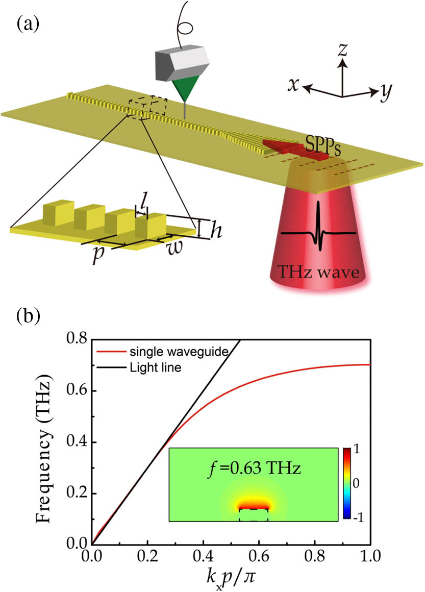
Surface plasmon polaritons (SPPs) with the features of subwavelength confinement and strong enhancements have sparked enormous interest. However, in the terahertz regime, due to the perfect conductivities of most metals, it is hard to realize the strong confinement of SPPs, even though the propagation loss could be sufficiently low. One main approach to circumvent this problem is to exploit spoof SPPs, which are expected to exhibit useful subwavelength confinement and relative low propagation loss at terahertz frequencies. Here we report the design, fabrication, and characterization of terahertz spoof SPP waveguides based on corrugated metal surfaces. The various waveguide components, including a straight waveguide, an S-bend waveguide, a Y-splitter, and a directional coupler, were experimentally demonstrated using scanning near-field terahertz microscopy. The proposed waveguide indeed enables propagation, bending, splitting, and coupling of terahertz SPPs and thus paves a new way for the development of flexible and compact plasmonic circuits operating at terahertz frequencies.
Integrated optics devices Surface waves Far infrared or terahertz Photonics Research
2018, 6(1): 01000018


